DATA CENTER REVOLUTION: SILICON PHOTONICS & CPO
The distinction between the electronic machine and its optical communications system begins to shrink. NVIDIA's latest CPO networking systems illustrate the direction.

– 7 min read
The distinction between the electronic machine and its optical communications system begins to shrink. NVIDIA's latest CPO networking systems illustrate the direction.
AI has created an unusual problem for the modern data center. The processors themselves have become extraordinarily powerful, but increasingly the difficulty is not simply performing calculations. It is moving the enormous quantities of information those processors require.
A large AI model may be distributed across hundreds, thousands or eventually tens of thousands of accelerators. Those processors cannot work independently. During training, and increasingly during large-scale inference, they continually exchange model states, activations and other numerical data. Memory must feed processors; processors must communicate with other processors; racks must communicate with other racks; clusters may need to communicate across entire data-center campuses.
The result is that the AI machine increasingly encounters its own internal communication system as a bottleneck.
This is where silicon photonics and co-packaged optics (CPO) become important.
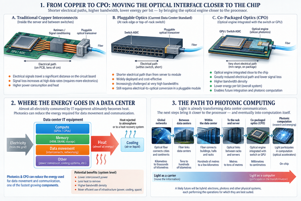
The underlying problem is relatively easy to understand. Electronic processors manipulate information electrically. Over short distances, copper remains extremely effective. It is inexpensive, mature, robust and requires no conversion from electrical signals into light. NVIDIA itself continues to use copper for short-range connections such as those inside racks.
But as bandwidth increases and distances become longer, electrical interconnects become progressively more difficult. Resistance, capacitive loading and frequency-dependent signal distortion constrain how far increasingly fast electrical signals can travel without substantial energy being spent maintaining signal integrity. A major 2026 Nature Electronics review identifies precisely these effects as fundamental limitations emerging in high-performance computing and AI interconnects. (Nature)
The traditional answer has been to convert the electrical data into light.
That is already what happens throughout the world's telecommunications infrastructure.
A laser provides an optical carrier. The information is encoded into properties of that light, transported through optical fiber and eventually converted back into an electrical signal.
For long distances, this is extraordinarily effective.
The problem inside the data center is where that conversion occurs.
In a conventional architecture, the processor or networking ASIC may sit some distance electrically from a pluggable optical transceiver at the edge of the system.
The data therefore has to travel electrically across a circuit board before reaching the optical module.
As speeds rise, that short electrical journey becomes increasingly expensive.
The signal deteriorates. Additional electronics—often including high-speed SerDes and digital signal processing—are required to preserve or reconstruct it. Those electronics consume electricity.
And electricity ultimately becomes heat.
Broadcom describes precisely this problem: as signaling rates increase, electrical path losses between an ASIC and conventional pluggable optical modules increase, requiring increasingly powerful electronics to compensate. (Broadcom)
The obvious question becomes:
Why make the electrical signal travel so far before turning it into light?
Move the optics closer.
That is the central idea behind co-packaged optics.
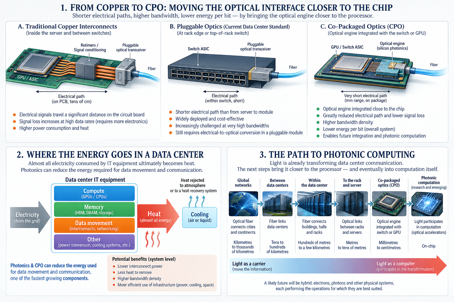
Instead of locating optical transceivers relatively far from the switching chip, CPO integrates the photonic components extremely close to the electronic ASIC—on the same package or closely integrated substrate.
Schematically:
Conventional architecture
GPU/ASIC
↓
electrical SerDes
↓
PCB copper traces
↓
pluggable optical transceiver
↓
fiber
↓
pluggable transceiver
↓
electrical path
↓
GPU/ASIC
With CPO:
GPU/ASIC
↓
nearby optical engine
↓
fiber
↓
nearby optical engine
↓
GPU/ASIC
The difference might look small on paper.
At hundreds of gigabits per second per channel, multiplied across enormous AI clusters, it is not small at all.
The electrical path becomes shorter. Signal losses fall. Some retiming and signal-conditioning requirements can be eliminated. Bandwidth density rises, and less electrical energy has to be spent merely getting information from the chip to the fiber.
This is why CPO is becoming so important to AI infrastructure. A recent Nature Electronics review describes a technological roadmap extending from present two-dimensional CPO toward 2.5-D integration and eventually three-dimensional heterogeneous stacking of electronic and photonic components. (Nature)
In other words:
the fiber is moving toward the processor.
This becomes possible partly because optical components themselves can increasingly be fabricated using semiconductor manufacturing techniques.
Silicon photonics places microscopic optical structures—waveguides, modulators and other photonic components—onto chips.
A conventional electrical chip guides electrons through conductive pathways.
A photonic integrated circuit can guide light through microscopic waveguides.
Instead of a fiber-optic cable being something that begins several centimetres or metres away from the processor, optical pathways increasingly become part of the processor's immediate physical environment.
The distinction between the electronic machine and its optical communications system begins to shrink.
NVIDIA's latest CPO networking systems illustrate the direction. The company says its silicon-photonic CPO switches can achieve substantially better networking power efficiency than conventional pluggable-transceiver architectures and eliminate some DSP retiming requirements. Its Spectrum-X photonic systems are designed around aggregate switching bandwidth reaching hundreds of terabits per second. Those figures are vendor claims rather than universal characteristics of CPO, but they show why the industry is investing so heavily in the technology. (NVIDIA)
And NVIDIA's commitment is hardly theoretical. In March 2026 it announced a multiyear partnership with Coherent, including a $2 billion investment, aimed at expanding laser and advanced-optics capacity for future AI infrastructure. (NVIDIA Newsroom)
An important distinction must be made.
CPO uses photons primarily to move information.
The GPUs are still electronic computers.
The matrix multiplications are still overwhelmingly performed electronically. Memory remains predominantly electronic. The optical system transports the information from one electronic computational component to another.
So:
electronic computation → optical communication → electronic computation.
But once light has penetrated this deeply into the computing architecture, another question becomes difficult to avoid.
Why convert it back?
Light doesn't merely travel.
Optical waves interact.
They interfere.
They possess amplitude and phase.
Different wavelengths can coexist within the same physical pathway.
Those properties can themselves represent and transform numerical relationships.
And neural networks happen to depend heavily upon mathematical operations—particularly large linear-algebra operations such as matrix and vector transformations—that can in principle be mapped onto optical systems.
Instead of instructing electronic transistors to perform every individual multiply-and-add operation sequentially or in electronic parallelism, a photonic structure can sometimes be arranged so that the propagation and interference of light performs the mathematical transformation physically.
That represents a much deeper transition.
We move from:
using light to carry the numbers
toward:
using light to participate in transforming the numbers.
Photonic AI accelerators are already an active research field. A Nature Photonics assessment published on September 15 concludes that photonic accelerators are becoming a viable route toward more sustainable AI, while emphasizing that optical loss, electro-optical conversion, scalability, nonlinear operations and reconfigurability remain substantial obstacles. (Nature)
So we should not imagine an imminent all-optical replacement for GPUs.
But the trajectory is real.
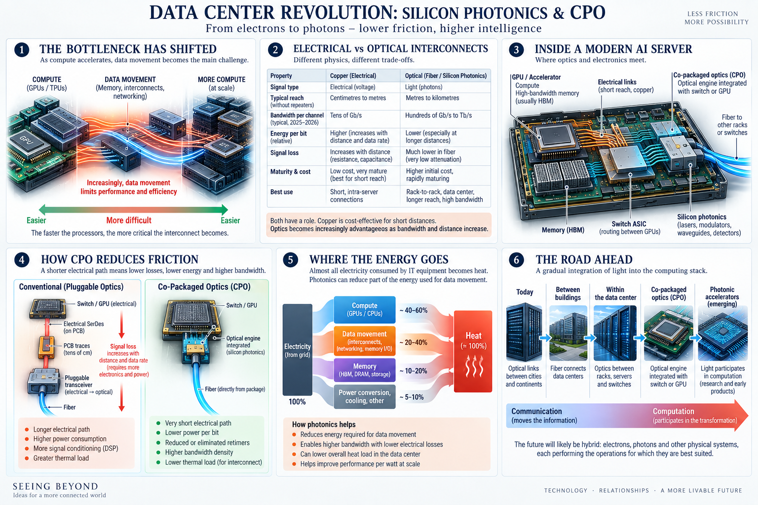
We can now see several stages in the development:
Stage 1 — Copper communication
Electronic processors communicate electrically.
Stage 2 — Optical long-distance networking
Fiber carries information between cities, countries and data centers.
Stage 3 — Optical data-center networking
Fiber increasingly connects switches, racks and clusters.
Stage 4 — Co-packaged optics
The electro-optical boundary moves toward the processor itself.
Stage 5 — Optical I/O and photonic integration
Optical pathways become increasingly integrated with the computing package.
Stage 6 — Photonic acceleration
Light begins performing selected mathematical transformations.
And perhaps eventually:
Stage 7 — Hybrid computational architectures
Electrons, photons, analog devices and other physical systems each perform the operations for which their physical properties are best suited.
This last possibility may ultimately matter more than the idea of an entirely photonic computer.
The future computer may not speak one physical language.
There is another important lesson here.
We often imagine the energy consumption of AI as the cost of calculation.
Increasingly, however, a major part of the challenge is communication.
A processor cannot calculate with information it does not possess.
Model weights have to arrive.
Activations have to arrive.
Results have to leave.
Thousands of processors have to coordinate their work.
At sufficiently large scale, processors can actually spend time waiting for information from other processors.
Recent research into parallel photonic integration explicitly attacks this problem. An August 2026 Nature Communications paper investigated optical approaches to collective communication operations across large accelerator clusters—the kind of operations required when many processors must exchange and combine information. (Nature)
This suggests a useful reformulation:
The future of AI efficiency may depend as much upon reducing the cost of moving intelligence's representations as upon reducing the cost of calculating with them.
And that brings us back to heat.
Electrical resistance is not the only source of heat in a data center. Transistor switching, capacitance, leakage, memory operations, voltage conversion, networking and many other processes consume energy.
But almost all the electricity entering the electronic system ultimately becomes heat.
So shortening an electrical pathway doesn't merely improve communication.
At enormous scale it can mean:
less electrical energy → less heat → less cooling → potentially less water → less infrastructure.
This is why silicon photonics isn't simply about making AI faster.
It is potentially part of reducing the physical footprint of AI.
Yet optics isn't frictionless.
Lasers consume electricity.
Modulators require energy.
Photodetectors have losses.
Optical signals attenuate.
Converting between photons and electrons consumes energy.
Packaging microscopic optical and electronic systems together creates formidable manufacturing and thermal problems.
Indeed, current research identifies the electro-optical boundary itself as one of the central challenges. (Nature)
That makes the direction particularly interesting.
If conversion creates friction, one response is not merely to make conversion more efficient.
It is to ask whether conversion needs to occur so frequently.
This may be the most useful way to understand the silicon-photonics revolution.
It isn't simply:
replace copper with fiber.
It is:
move the boundary between electronics and optics.
Originally that boundary sat kilometres away.
Then metres.
Then centimetres.
With CPO, optics approaches the switching silicon itself.
With photonic computing, the boundary potentially moves inside computation.
And every time that boundary moves, we can ask:
What physical work have we eliminated?
That question is more interesting than simply asking whether the new system is faster.
Because the fundamental challenge confronting AI infrastructure is no longer merely computation.
It is the enormous physical machinery required to instantiate computation at scale.
The processors.
The memory.
The networking.
The electricity.
The heat.
The cooling.
The water.
The substations.
The power plants.
Silicon photonics and co-packaged optics do not eliminate those requirements.
But they demonstrate an important principle:
instead of continually expanding the infrastructure required to accommodate AI, we can also reconsider the physical architecture that created those requirements.
Perhaps the data-center revolution will therefore not ultimately be measured by how many more GPUs we can place inside a building.
It may be measured by how much of the machinery between information and transformation we learn to remove.